
To adapt to the growing international emphasis on environmental protection, PCBA has been changed from lead-based processes to lead-free processes, and new laminate materials have been applied. These changes will all cause changes in the solder joint performance of PCB electronic products. Since the solder joints of components are very sensitive to strain failure, it is crucial to understand the strain characteristics of PCB electronic products under the worst conditions through strain testing.
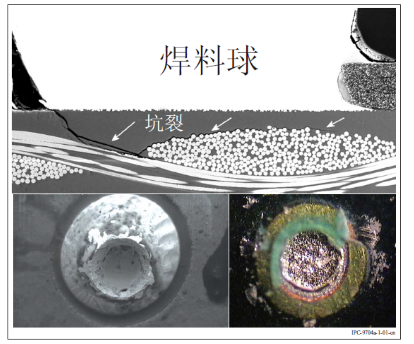
For different solder alloys, package types, surface treatments or laminate materials, excessive strain can lead to failures in various modes. Failures include solder ball cracking, line damage, laminate-related adhesive failure (pad lifting) or cohesive failure (pad cratering) and package substrate cracking (see Figure 1-1). It has been verified that using strain measurement to control printed board warpage is beneficial to the electronics industry, and it is gradually being recognized as a method to identify and improve production operations.
Strain testing can objectively analyze the strain and strain rate levels of SMT packages during PCBA assembly, testing and operation, providing a quantitative method for printed board warpage measurement and risk level assessment.
The goal of strain measurement is to characterize all assembly steps involving mechanical loads.
Post time: Oct-18-2024


