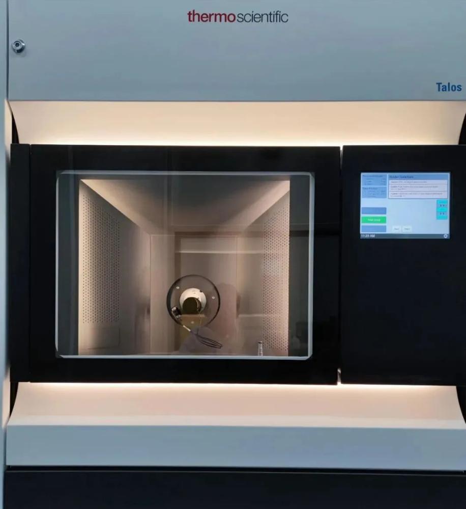
Transmission Electron Microscope (TEM) is a microphysical structure analysis technique based on electron microscopy based on electron beam as a light source, with a maximum resolution of about 0.1nm. The emergence of TEM technology has greatly improved the limit of human naked eye observation of microscopic structures, and is an indispensable microscopic observation equipment in the semiconductor field, and is also an indispensable equipment for process research and development, mass production process monitoring, and process anomaly analysis in the semiconductor field.
TEM has a very wide range of applications in the semiconductor field, such as wafer manufacturing process analysis, chip failure analysis, chip reverse analysis, coating and etching semiconductor process analysis, etc., the customer base is all over the fabs, packaging plants, chip design companies, semiconductor equipment research and development, material research and development, university research institutes and so on.
GRGTEST TEM Technical team capability introduction
The TEM technical team is led by Dr. Chen Zhen, and the technical backbone of the team has more than 5 years of experience in related industries. They not only have rich experience in TEM result analysis, but also rich experience in FIB sample preparation, and have the ability to analyze 7nm and above advanced process wafers and the key structures of various semiconductor devices. At present, our customers are all over the domestic first-line fabs, packaging factories, chip design companies, universities and scientific research institutes, etc., and are widely recognized by customers.
Post time: Apr-13-2024


